Organic Transistors and Complementary Circuits
This page describes a previous research project. Read about our current work here.
Stuart undertook his PhD research in the lab of Professor Alasdair Campbell at Imperial College London, from 2010 to 2014. He developed high-speed organic transistors and complementary circuits on plastic. His work used a combination of multiple types of lithography, gravure and inkjet printing.
Listen to Stuart talk about the use of lithography and graphics arts methods in electronics on the podcast Handmade with Dr Anna Ploszajski:
Self-aligned, megahertz switching organic transistors
Stuart developed a high-performance organic transistor architecture to overcome the relatively low charge mobilities of conjugated polymers compared to silicon. This allowed the transistors to operate at frequencies sufficient for applications such as flexible displays.
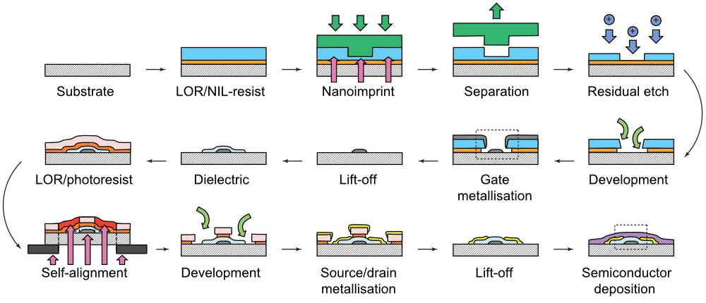
Stuart was trained in the use of nanoimprint- and self-aligned lithography by the team of Dr Barbara Stadlober at Joanneum Research, Austria. He brought these processes back to Imperial College to build devices with sub-micron channel lengths and electrode overlaps. This resulted in organic transistors operating at megahertz frequencies, amongst the fastest achieved at the time of reporting.1
Read about the process flow developed to enable megahertz-operating organic transistors
Gravure and inkjet printed complementary circuits
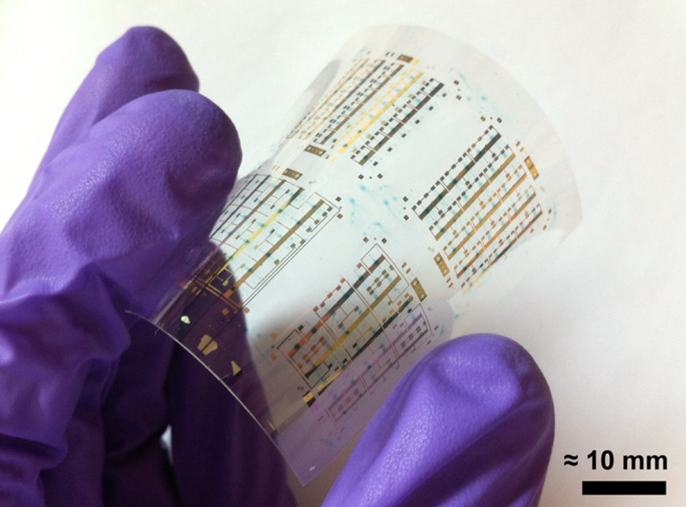
Stuart combined his transistor architectures with gravure and inkjet printing to create complementary circuits. In collaboration with the team of Dr Mario Caironi at Istituto Italiano di Tecnologia, Milan, they were able to measure NAND and NOR complementary logic gates for a variety of fabrication permutations.
This systematic study allowed them to evaluate different fabrication techniques and their impact on electrical performance.2
Read about gravure and inkjet printed complementary circuits
Image analysis of gravure printed device layers
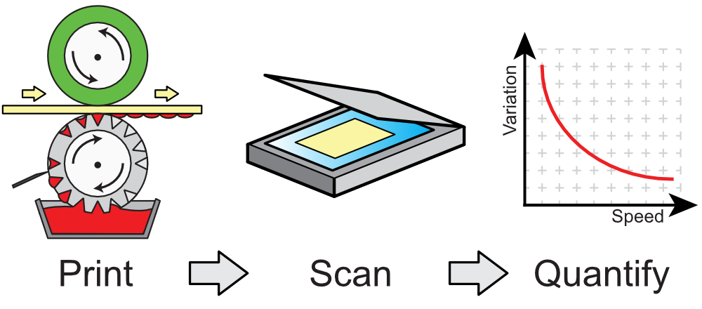
The large parameter space of printing processes make them challenging to optimise. Stuart developed an image analysis pipeline to quantitatively assess the quality of gravure printed components in the device stack, as part of the MSci project of Dr Francesa Boughey and Russell Hills. This approach allowed us to effectively optimise the device printing process.3
Read our publication on optimising gravure printed organic semiconductors
-
Reproduced under terms of CC-BY license from: Higgins SG, Muir BVO, Wade J, Chen J, Striedinger B, Gold H, Stadlober B, Caironi M, Kim J-S, Steinke JHG, Campbell AJ, Organic Transistors: Self-Aligned Megahertz Organic Transistors Solution-Processed on Plastic, 2015, Advanced Electronic Materials, DOI: 10.1002/aelm.201570013 ↩
-
Reproduced under terms of CC-BY license from: Higgins SG, Muir BVO, Heeney M, Campbell AJ, Indacenodithiophene–Benzothiadiazole Organic Field-Effect Transistors with Gravure-Printed Semiconductor and Dielectric on Plastic, 2015, MRS Communications, DOI: 10.1557/mrc.2015.66 ↩
-
Reproduced under terms of CC-BY license from: Higgins SG, Boughey FL, Hills R, Steinke JHG, Muir BVO, Campbell AJ, Quantitative Analysis and Optimization of Gravure Printed Metal Ink, Dielectric, and Organic Semiconductor Films, 2015, ACS Applied Materials & Interfaces, DOI: 10.1021/am508316f ↩


